ICGOO在线商城 > TLE42744G V50
 Datasheet下载
- 型号: TLE42744G V50
- 制造商: Infineon
- 库位|库存: xxxx|xxxx
- 要求:
| 数量阶梯 | 香港交货 | 国内含税 |
| +xxxx | $xxxx | ¥xxxx |
查看当月历史价格
查看今年历史价格
TLE42744G V50产品简介:
ICGOO电子元器件商城为您提供TLE42744G V50由Infineon设计生产,在icgoo商城现货销售,并且可以通过原厂、代理商等渠道进行代购。 提供TLE42744G V50价格参考以及InfineonTLE42744G V50封装/规格参数等产品信息。 你可以下载TLE42744G V50参考资料、Datasheet数据手册功能说明书, 资料中有TLE42744G V50详细功能的应用电路图电压和使用方法及教程。
| 参数 | 数值 |
| 产品目录 | 集成电路 (IC)半导体 |
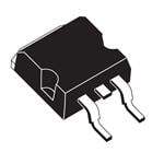
| 描述 | IC REG LDO 5V 0.4A TO263-3低压差稳压器 LINEAR VLTGE REG |
| 产品分类 | |
| 品牌 | Infineon Technologies |
| 产品手册 | http://www.infineon.com/dgdl/TLE42744_DS_11.pdf?folderId=db3a304318f3fe290118f5a433570040&fileId=db3a304327b897500128012ccafe37d2 |
| 产品图片 |
|
| rohs | 符合RoHS无铅 / 符合限制有害物质指令(RoHS)规范要求 |
| 产品系列 | 电源管理 IC,低压差稳压器,Infineon Technologies TLE42744G V50- |
| 数据手册 | http://www.infineon.com/dgdl/TLE42744-Data-Sheet-12-Infineon.pdf?folderId=db3a304318f3fe290118f5a433570040&fileId=db3a304327b897500128012ccafe37d2&ack=t |
| 产品型号 | TLE42744G V50 |
| PCN设计/规格 | |
| PSRR/纹波抑制—典型值 | 60 dB |
| 产品 | LDO Voltage Regulators |
| 产品种类 | 低压差稳压器 |
| 供应商器件封装 | PG-TO263-3 |
| 其它名称 | SP000463264 |
| 包装 | 带卷 (TR) |
| 商标 | Infineon Technologies |
| 回动电压—最大值 | 500 mV |
| 安装类型 | 表面贴装 |
| 安装风格 | SMD/SMT |
| 封装 | Reel |
| 封装/外壳 | TO-263-4,D²Pak(3 引线+接片),TO-263AA |
| 封装/箱体 | TO-263-3 |
| 工作温度 | -40°C ~ 150°C |
| 工厂包装数量 | 1000 |
| 最大工作温度 | + 150 C |
| 最大输入电压 | 40 V |
| 最小工作温度 | - 40 C |
| 最小输入电压 | 5.5 V |
| 标准包装 | 1,000 |
| 电压-跌落(典型值) | 0.25V @ 250mA |
| 电压-输入 | 5.5 V ~ 40 V |
| 电压-输出 | 5V |
| 电流-输出 | 400mA |
| 电流-限制(最小值) | 400mA |
| 稳压器拓扑 | 正,固定式 |
| 稳压器数 | 1 |
| 系列 | TLE42744 |
| 线路调整率 | 25 mV |
| 负载调节 | 50 mV |
| 输出电压 | 5 V |
| 输出电流 | 400 mA |
| 输出端数量 | 1 Output |
| 输出类型 | Fixed |
| 零件号别名 | SP000463264 TLE42744GV50ATMA1 |


- 商务部:美国ITC正式对集成电路等产品启动337调查
- 曝三星4nm工艺存在良率问题 高通将骁龙8 Gen1或转产台积电
- 太阳诱电将投资9.5亿元在常州建新厂生产MLCC 预计2023年完工
- 英特尔发布欧洲新工厂建设计划 深化IDM 2.0 战略
- 台积电先进制程称霸业界 有大客户加持明年业绩稳了
- 达到5530亿美元!SIA预计今年全球半导体销售额将创下新高
- 英特尔拟将自动驾驶子公司Mobileye上市 估值或超500亿美元
- 三星加码芯片和SET,合并消费电子和移动部门,撤换高东真等 CEO
- 三星电子宣布重大人事变动 还合并消费电子和移动部门
- 海关总署:前11个月进口集成电路产品价值2.52万亿元 增长14.8%


PDF Datasheet 数据手册内容提取
TLE42744 Low Dropout Linear Voltage Regulator TLE42744DV50 TLE42744GV50 TLE42744EV50 TLE42744GV33 TLE42744DV33 TLE42744GSV33 Data Sheet Rev. 1.3, 2018-03-05 Automotive Power
Low Dropout Linear Voltage Regulator TLE42744 1 Overview Features • Very Low Current Consumption • Output Voltages 5V and 3.3V ±2% • Output Current up to 400mA PG-TO252-3 PG-SSOP-14 exposed pad • Very Low Dropout Voltage • Output Current Limitation • Reverse Polarity Protection • Overtemperature Shutdown • Wide Temperature Range From -40°C up to 150°C • Green Product (RoHS compliant) • AEC Qualified PG-TO263-3 PG-SOT223-4 Description The TLE42744 is a monolithic integrated low dropout voltage regulator for load currents up to 400mA. An input voltage up to 40 V is regulated to V =5V/3.3V with a precision of ±2%. The device is designed for the harsh Q,nom environment of automotive applications. Therefore it is protected against overload, short circuit and overtemperature conditions by the implemented output current limitation and the overtemperature shutdown circuit. The TLE42744 can be also used in all other applications requiring a stabilized 5V/3.3V voltage. Due to its very low quiescent current the TLE42744 is dedicated for use in applications permanently connected to V . BAT Type Package Marking TLE42744DV50 PG-TO252-3 42744V5 TLE42744GV50 PG-TO263-3 42744V5 TLE42744EV50 PG-SSOP-14 exposed pad 42744V5 TLE42744DV33 PG-TO252-3 4274433 TLE42744GV33 PG-TO263-3 42744V33 TLE42744GSV33 PG-SOT223-4 427443 Data Sheet 2 Rev. 1.3, 2018-03-05
TLE42744 Block Diagram 2 Block Diagram Temperature Saturation Control and Sensor Protection Circuit Ι Q Control Amplifier Buffer Bandgap Reference GND AEB01959 Figure1 Block Diagram Data Sheet 3 Rev. 1.3, 2018-03-05
TLE42744 Pin Configuration 3 Pin Configuration 3.1 Pin Assignment PG-TO252-3, PG-TO263-3 and PG-SOT223-4 GND GND 4 1 3 1 2 3 I GND Q Ι Q Ι GND Q PinConfig_PG-SOT42.v2sd3- AEP02561 AEP02281 Figure2 Pin Configuration (top view) 3.2 Pin Definitions and Functions PG-TO252-3, PG-TO263-3 and PG-SOT223-4 Pin No. Symbol Function 1 I Input block to ground directly at the IC with a ceramic capacitor 2 GND Ground internally connected to heat slug 3 Q Output block to ground with a capacitor close to the IC terminals, respecting the values given for its capacitance and ESR in “Functional Range” on Page6 4 / Heat Slug – Heat Slug internally connected to GND; connect to GND and heatsink area Data Sheet 4 Rev. 1.3, 2018-03-05
TLE42744 Pin Configuration 3.3 Pin Assignment PG-SSOP-14 exposed pad n.c. 1 14 n.c. n.c. 2 13 I n.c. 3 12 n.c. GND 4 11 n.c. n.c. 5 10 n.c. n.c. 6 9 Q n.c. 7 8 n.c. TLE7274-2_PINCONFIG_SSOP- 14.SVG Figure3 Pin Configuration (top view) 3.4 Pin Definitions and Functions PG-SSOP-14 exposed pad Pin No. Symbol Function 1, 2, 3, 5, 6, 7 n.c. Not connected can be open or connected to GND 4 GND Ground 8, 10, 11, 12, n.c. Not connected 14 can be open or connected to GND 9 Q Output block to ground with a capacitor close to the IC terminals, respecting the values given for its capacitance and ESR in “Functional Range” on Page6 13 I Input block to ground directly at the IC with a ceramic capacitor Pad – Exposed Pad connect to GND and heatsink area Data Sheet 5 Rev. 1.3, 2018-03-05
TLE42744 General Product Characteristics 4 General Product Characteristics 4.1 Absolute Maximum Ratings Table1 Absolute Maximum Ratings1) T =-40°C to 150 °C; all voltages with respect to ground, (unless otherwise specified) j Parameter Symbol Values Unit Note / TestCondition Number Min. Typ. Max. Input I Voltage V -42 – 45 V – P_4.1.1 I Output Q Voltage V -1 – 40 V – P_4.1.2 Q Temperature Junction temperature T -40 – 150 °C – P_4.1.3 j Storage temperature T -50 – 150 °C – P_4.1.4 stg ESD Susceptibility ESD Absorption V -4 – 4 kV Human Body Model P_4.1.5 ESD,HBM (HBM)2) ESD Absorption V -1000 – 1000 V Charge Device Model P_4.1.6 ESD,CDM (CDM)3) at all pins 1) not subject to production test, specified by design 2) ESD susceptibility Human Body Model “HBM” according to AEC-Q100-002 - JESD22-A114 3) ESD susceptibility Charged Device Model “CDM” according to ESDA STM5.3.1 Notes 1. Stresses above the ones listed here may cause permanent damage to the device. Exposure to absolute maximum rating conditions for extended periods may affect device reliability. 2. Integrated protection functions are designed to prevent IC destruction under fault conditions described in the data sheet. Fault conditions are considered as “outside” normal operating range. Protection functions are not designed for continuous repetitive operation. 4.2 Functional Range Table2 Functional Range Parameter Symbol Values Unit Note / TestCondition Number Min. Typ. Max. Input voltage V 5.5 – 40 V TLE42744DV50, P_4.2.1 I TLE42744GV50, TLE42744EV50 Input voltage V 4.7 – 40 V TLE42744GV33, P_4.2.2 I TLE42744DV33, TLE42744GSV33 Data Sheet 6 Rev. 1.3, 2018-03-05
TLE42744 General Product Characteristics Table2 Functional Range (cont’d) Parameter Symbol Values Unit Note / TestCondition Number Min. Typ. Max. Output Capacitor’s C 22 – µF 1) P_4.2.3 Q Requirements for Stability Output Capacitor’s ESR(C ) – 3 Ω 2) P_4.2.4 Q Requirements for Stability Junction temperature T -40 150 °C – P_4.2.5 j 1) the minimum output capacitance requirement is applicable for a worst case capacitance tolerance of 30% 2) relevant ESR value at f=10kHz Note:Within the functional or operating range, the IC operates as described in the circuit description. The electrical characteristics are specified within the conditions given in the Electrical Characteristics table. 4.3 Thermal Resistance Note:This thermal data was generated in accordance with JEDEC JESD51 standards. For more information, go to www.jedec.org. Table3 Thermal Resistance Parameter Symbol Values Unit Note / TestCondition Number Min. Typ. Max. TLE42744DV50, TLE42744DV33 (PG-TO252-3) Junction to Case1) R – 3.6 – K/W measured to heat slug P_4.3.1 thJC Junction to Ambient1) R – 27 – K/W FR4 2s2p board2) P_4.3.2 thJA Junction to Ambient1) R – 115 – K/W FR4 1s0p board, P_4.3.3 thJA footprint only3) Junction to Ambient1) R – 52 – K/W FR4 1s0p board, P_4.3.4 thJA 300mm² heatsink area3) Junction to Ambient1) R – 40 – K/W FR4 1s0p board, P_4.3.5 thJA 600mm² heatsink area3) TLE42744GV50, TLE42744GV33 (PG-TO263-3) Junction to Case1) R – 3.6 – K/W measured to heat slug P_4.3.6 thJC Junction to Ambient1) R – 22 – K/W FR4 2s2p board2) P_4.3.7 thJA Junction to Ambient1) R – 74 – K/W FR4 1s0p board, P_4.3.8 thJA footprint only3) Junction to Ambient1) R – 42 – K/W FR4 1s0p board, P_4.3.9 thJA 300mm² heatsink area3) Junction to Ambient1) R – 34 – K/W FR4 1s0p board, P_4.3.10 thJA 600mm² heatsink area3) Data Sheet 7 Rev. 1.3, 2018-03-05
TLE42744 General Product Characteristics Table3 Thermal Resistance (cont’d) Parameter Symbol Values Unit Note / TestCondition Number Min. Typ. Max. TLE42744EV50 (PG-SSOP-14 exposed pad) Junction to Case1) R – 7 – K/W measured to exposed P_4.3.11 thJC pad Junction to Ambient1) R – 43 – K/W FR4 2s2p board2) P_4.3.12 thJA Junction to Ambient1) R – 120 – K/W FR4 1s0p board, P_4.3.13 thJA footprint only3) Junction to Ambient1) R – 59 – K/W FR4 1s0p board, P_4.3.14 thJA 300mm² heatsink area3) Junction to Ambient1) R – 49 – K/W FR4 1s0p board, P_4.3.15 thJA 600mm² heatsink area3) TLE42744GSV33 (PG-SOT223-4) Junction to Case1) R – 17 – K/W measured to heat slug P_4.3.16 thJC Junction to Ambient1) R – 54 – K/W FR4 2s2p board2) P_4.3.17 thJA Junction to Ambient1) R – 139 – K/W FR4 1s0p board, P_4.3.18 thJA footprint only3) Junction to Ambient1) RthJA – 73 – K/W FR4 1s0p board, P_4.3.19 300mm² heatsink area3) Junction to Ambient1) R – 64 – K/W FR4 1s0p board, P_4.3.20 thJA 600mm² heatsink area3) 1) Not subject to production test, specified by design. 2) Specified R value is according to Jedec JESD51-2,-5,-7 at natural convection on FR4 2s2p board; The Product thJA (Chip+Package) was simulated on a 76.2 x 114.3 x 1.5 mm³ board with 2 inner copper layers (2 x 70µm Cu, 2 x 35µm Cu). Where applicable a thermal via array under the exposed pad contacted the first inner copper layer. 3) Specified R value is according to Jedec JESD 51-3 at natural convection on FR4 1s0p board; The Product thJA (Chip+Package) was simulated on a 76.2 × 114.3 × 1.5 mm3 board with 1 copper layer (1 x 70µm Cu). Data Sheet 8 Rev. 1.3, 2018-03-05
TLE42744 Electrical Characteristics 5 Electrical Characteristics 5.1 Electrical Characteristics Voltage Regulator Table4 Electrical Characteristics V =13.5 V; T =-40°C to 150 °C; all voltages with respect to ground (unless otherwise specified) I j Parameter Symbol Values Unit Note / TestCondition Number Min. Typ. Max. Output Q Output Voltage V 4.9 5.0 5.1 V TLE42744DV50, P_5.1.1 Q TLE42744GV50, TLE42744EV50 5mA<I <400mA Q 6V<V <28V I Output Voltage V 4.9 5.0 5.1 V TLE42744DV50, P_5.1.2 Q TLE42744GV50, TLE42744EV50 5mA<I <200mA Q 6V<V <40V I Output Voltage V 3.23 3.3 3.37 V TLE42744GV33, P_5.1.3 Q TLE42744DV33, TLE42744GSV33; 5mA<I <400mA Q 4.7V<V <28V I Output Voltage V 3.23 3.3 3.37 V TLE42744GV33, P_5.1.4 Q TLE42744DV33, TLE42744GSV33; 5mA<I <200mA Q 4.7V<V <40V I Dropout Voltage V – 250 500 mV TLE42744DV50, P_5.1.5 dr TLE42744GV50, TLE42744EV50 I =250mA Q V =V –V 1) dr I Q Load Regulation ∆V – 20 50 mV TLE42744DV50, P_5.1.6 Q, lo TLE42744GV50, TLE42744EV50; I =5mA to 400mA Q V =6V I Load Regulation ∆V – 40 70 mV TLE42744GV33, P_5.1.7 Q, lo TLE42744DV33, TLE42744GSV33; I =5mA to 300mA Q Line Regulation ∆V – 10 25 mV V =12V to 32V P_5.1.8 Q, li l I =5mA Q Data Sheet 9 Rev. 1.3, 2018-03-05
TLE42744 Electrical Characteristics Table4 Electrical Characteristics (cont’d) V =13.5 V; T =-40°C to 150 °C; all voltages with respect to ground (unless otherwise specified) I j Parameter Symbol Values Unit Note / TestCondition Number Min. Typ. Max. Output Current Limitation I 400 600 1100 mA 1) P_5.1.9 Q Power Supply Ripple Rejection2) PSRR – 60 – dB f =100Hz; V =0.5Vpp P_5.1.10 r r Temperature Output Voltage dV – 0.5 – mV/K – P_5.1.11 --------Q--- Drift dT Overtemperature Shutdown T 151 – 200 °C T increasing2) P_5.1.12 j,sd j Threshold Overtemperature Shutdown T – 25 – °C T decreasing2) P_5.1.13 j,sdh j Threshold Hysteresis Current Consumption Quiescent Current I – 100 220 µA I =1mA P_5.1.14 q Q I =I –I q I Q Current Consumption I – 8 15 mA I =250mA P_5.1.15 q Q I =I –I q I Q Current Consumption I – 15 25 mA TLE42744DV50, P_5.1.16 q I =I –I TLE42744GV50, q I Q TLE42744EV50; I =400mA Q Current Consumption I – 20 30 mA TLE42744GV33, P_5.1.17 q I =I –I TLE42744DV33, q I Q TLE42744GSV33; I =400mA Q 1) Measured when the output voltage V has dropped 100 mV from the nominal value obtained at V = 13.5 V. Q I 2) not subject to production test, specified by design Data Sheet 10 Rev. 1.3, 2018-03-05
TLE42744 Electrical Characteristics 5.2 Typical Performance Characteristics Voltage Regulator Current Consumption I versus Current Consumption I versus q q Output Current I Low Output Current I Q Q 16 01_IQ_IQ.VSD 1,4 02_IQ_IQLOW.VSD 14 1,2 12 VI = 13.5 V VI = 13.5 V Tj = 25 °C 1 Tj = 25 °C 10 A] A] 0,8 m 8 m [q [q 0,6 I I 6 0,4 4 2 0,2 0 0 0 100 200 300 400 0 20 40 60 80 100 IQ [mA] IQ [mA] Output Voltage Variation ∆V versus Dropout Voltage V versus Q dr Junction Temperature T Output Current I (5V versions only) J Q 03_VQ_TJ.VSD 0,5 500 04_VDR_IQ.VSD T = 150 °C 0,4 450 j IQ = 5 mA T = 25 °C j 0,3 V = 13.5 V 400 I T = -40 °C j 0,2 350 %] 0,1 V] 300 m [Q 0 [R 250 V D Δ -0,1 V 200 -0,2 150 -0,3 100 -0,4 50 -0,5 0 -40 0 40 80 120 150 0 100 200 300 400 I [mA] T [°C] Q j Data Sheet 11 Rev. 1.3, 2018-03-05
TLE42744 Electrical Characteristics Dropout Voltage V versus Maximum Output Current I versus dr Q Junction Temperature (5V versions only) Input Voltage V I 500 05_VDR_TJ.VSD 900 06_IQMAX_VI.VSD 450 800 400 700 T = 25 °C I = 400 mA j 350 Q 600 Tj = -40 °C ] 300 ] V A T = 150 °C j m m 500 [R 250 [x D ma 400 V 200 Q, I = 100 mA I 150 Q 300 100 200 I = 10 mA V =V - 100 mV 50 Q Q Q,nom 100 0 0 -40 0 40 80 120 160 0 10 20 30 40 Tj [°C] VI [V] Region Of Stability: Output Capacitor’s ESR ESR(C ) versus Output Current I Q Q 10 07_ESR_IQ.VSD Unstable Region ] 1 Ω [ Stable ) Q C = 22 µF Region Q C V = 13.5 V ( I R S 0,1 E 0,01 0 100 200 300 400 I [mA] Q Data Sheet 12 Rev. 1.3, 2018-03-05
TLE42744 Application Information 6 Application Information Note:The following information is given as a hint for the implementation of the device only and shall not be regarded as a description or warranty of a certain functionality, condition or quality of the device. 6.1 Application Diagram Regulated Supply II I Q IQ Output Voltage Current Limitation Load (e.g. DI CI2 CI1 CQ Micro Bandgap 22µF Controller) <45V 10µF 100nF Reference (ESR<3Ω) Temperature Shutdown GND GND Figure4 Application Diagram 6.2 Selection of External Components 6.2.1 Input Pin The typical input circuitry for a linear voltage regulator is shown in the application diagram above. A ceramic capacitor at the input, in the range of 100nF to 470nF, is recommended to filter out the high frequency disturbances imposed by the line e.g. ISO pulses 3a/b. This capacitor must be placed very close to the input pin of the linear voltage regulator on the PCB. An aluminum electrolytic capacitor in the range of 10µF to 470µF is recommended as an input buffer to smooth out high energy pulses, such as ISO pulse 2a. This capacitor should be placed close to the input pin of the linear voltage regulator on the PCB. An overvoltage suppressor diode can be used to further suppress any high voltage beyond the maximum rating of the linear voltage regulator and protect the device against any damage due to over-voltage. The external components at the input are not mandatory for the operation of the voltage regulator, but they are recommended in case of possible external disturbances. 6.2.2 Output Pin An output capacitor is mandatory for the stability of linear voltage regulators. The requirement to the output capacitor is given in “Functional Range” on Page6. The graph “Region Of Stability: Output Capacitor’s ESR ESR(CQ) versus Output Current IQ” on Page12 shows the stable operation range of the device. Data Sheet 13 Rev. 1.3, 2018-03-05
TLE42744 Application Information TLE42744 is designed to be stable with extremely low ESR capacitors. According to the automotive environment, ceramic capacitors with X5R or X7R dielectrics are recommended. The output capacitor should be placed as close as possible to the regulator’s output and GND pins and on the same side of the PCB as the regulator itself. In case of rapid transients of input voltage or load current, the capacitance should be dimensioned in accordance and verified in the real application that the output stability requirements are fulfilled. 6.3 Thermal Considerations Knowing the input voltage, the output voltage and the load profile of the application, the total power dissipation can be calculated: (1) P = (V –V )×I +V ×I D I Q Q I q with • P : continuous power dissipation D • V: input voltage I • V : output voltage Q • I : output current Q • I : quiescent current q The maximum acceptable thermal resistance R can then be calculated: thJA (2) T –T R = ----j--,--m----a--x-------------a- thJA,max P D with • T : maximum allowed junction temperature j,max • T : ambient temperature a Based on the above calculation the proper PCB type and the necessary heat sink area can be determined with reference to the specification in “Thermal Resistance” on Page7. Example Application conditions: V = 13.5V I V = 5V Q I = 250mA Q T = 85°C a Calculation of R : thJA,max P =(V – V ) • I + V • I D I Q Q I q =(13.5V – 5V) • 250mA + 13.5V • 15mA =2.125W + 0.2025W =2.3275W Data Sheet 14 Rev. 1.3, 2018-03-05
TLE42744 Application Information R =(T – T ) / P thJA,max j,max a D =(150°C – 85°C) / 2.3275W =27.93K/W As a result, the PCB design must ensure a thermal resistance R lower than 27.93K/W. By considering thJA TLE42744GV50 (PG-TO263-3 package) and according to “Thermal Resistance” on Page7, only the FR4 2s2p board is applicable. 6.4 Reverse Polarity Protection TLE42744 is self protected against reverse polarity faults and allows negative supply voltage. External reverse polarity diode is not needed. However, the absolute maximum ratings of the device as specified in “Absolute Maximum Ratings” on Page6 must be kept. The reverse voltage causes several small currents to flow into the IC hence increasing its junction temperature. As the thermal shut down circuitry does not work in the reverse polarity condition, designers have to consider this in their thermal design. Data Sheet 15 Rev. 1.3, 2018-03-05
TLE42744 Package Outlines 7 Package Outlines +0.15 6.5 -0.05 A +0.05 2.3 5.4 ±0.1 -0.10 (5) B 0.5 +0.08 -0.04 1 0. ± 1 +0.20 0.9 -0.01 ) 5 9.98±0.5 6.22-0.2 (4.24 0.8±0.1 0..N..0.15 MI 1 0.15 MAX. 5 3x 0. per side +0.08 0.75 ±0.1 0.5 -0.04 2.28 0.1 B 4.57 0.25 M A B All metal surfaces tin plated, except area of cut. GPT09277 Figure5 PG-TO252-3 Data Sheet 16 Rev. 1.3, 2018-03-05
TLE42744 Package Outlines 4.4 10±0.2 A 1.27±0.1 0...0.3 B 8.51) 0.1 3 0.05 0. ± 1 2 1) 2.4 ±0. 55 5) 25 7. (1 9. 5 0.3 ±0. 7± 7 2. 4. 0...0.15 0.75±0.1 0.5±0.1 1.05 2.54 8˚ MAX. 5.08 0.25 M A B 0.1 B 1) Typical All metal surfaces: tin plated, except area of cut. Metal surface min. x=7.25, y=6.9 GPT09362 Figure6 PG-TO263-3 Data Sheet 17 Rev. 1.3, 2018-03-05
TLE42744 Package Outlines 0.35 x 45° F 5 OF . 3.9±0.11) 0.1 H D 2x 0 X 0. D A 6 0.05± STAN (1.45) 1.7 M H +.01.09 X. 0 A M C 0.08 C ° 8 0.65 SEATING 0.64±0.25 PLANE 6 x 0.65 = 3.9 D 6±0.2 0.2 C 14x 2) 0.25±0.05 0.15 M C A-B D 14x Bottom View 3±0.2 A 14 8 1 7 0.2 ± 5 6 . 1 7 Exposed 14 8 2 B Diepad 0.1 H A-B 2x Index 1) Marking 4.9±0.1 1) Does not include plastic or metal protrusion of 0.15 max. per side 2) Lead width can be 0.61 max. in dambar area Figure7 PG-SSOP-14 exposed pad Data Sheet 18 Rev. 1.3, 2018-03-05
TLE42744 Package Outlines 6.5±0.2 1.6±0.1 A 3±0.1 0.1 MAX. 4 B 2 0.3 ±0. 7± N. 3.5 MI 5 1 2 3 0. 0.25M A 0.7±0.1 2.3 0.28±0.04 4.6 0.25M B 0...10˚ SOT223-PO V04 Figure8 PG-SOT223-4 Green Product (RoHS compliant) To meet the world-wide customer requirements for environmentally friendly products and to be compliant with government regulations the device is available as a green product. Green products are RoHS-Compliant (i.e Pb-free finish on leads and suitable for Pb-free soldering according to IPC/JEDEC J-STD-020). For further information on alternative packages, please visit our website: http://www.infineon.com/packages. Dimensions in mm Data Sheet 19 Rev. 1.3, 2018-03-05
TLE42744 Revision History 8 Revision History Revision Date Changes 1.3 2018-03-05 Marking update in Chapter Overview (TLE42744GSV33 and TLE42744DV33) Updated Template on the last page. 1.2 2014-07-03 Application Information added. PG-TO252-3 and PG-SSOP-14 EP package outlines updated. 1.1 2010-01-13 Updated Version Data Sheet: version TLE42744EV50 in PG-SSOP-14 exposed pad and all related description added; 3.3V versions TLE42744GV33 in PG-TO263-3, TLE42744DV33 in PG-TO252-3 and TLE42744GSV33 in PG-SOT223-4 and all related description added 1.0 2009-01-14 Initial Version final Data Sheet Data Sheet 20 Rev. 1.3, 2018-03-05
Trademarks All referenced product or service names and trademarks are the property of their respective owners. IMPORTANT NOTICE Edition 2018-03-05 The information given in this document shall in no For further information on technology, delivery terms event be regarded as a guarantee of conditions or and conditions and prices, please contact the nearest Published by characteristics ("Beschaffenheitsgarantie"). Infineon Technologies Office (www.infineon.com). Infineon Technologies AG With respect to any examples, hints or any typical 81726 Munich, Germany values stated herein and/or any information regarding the application of the product, Infineon Technologies WARNINGS hereby disclaims any and all warranties and liabilities © 2018 Infineon Technologies AG. of any kind, including without limitation warranties of Due to technical requirements products may contain All Rights Reserved. non-infringement of intellectual property rights of any dangerous substances. For information on the types third party. in question please contact your nearest Infineon In addition, any information given in this document is Technologies office. Do you have a question about any subject to customer's compliance with its obligations aspect of this document? stated in this document and any applicable legal Except as otherwise explicitly approved by Infineon Email: erratum@infineon.com requirements, norms and standards concerning Technologies in a written document signed by customer's products and any use of the product of authorized representatives of Infineon Technologies, Infineon Technologies in customer's applications. Infineon Technologies’ products may not be used in The data contained in this document is exclusively any applications where a failure of the product or any intended for technically trained staff. It is the consequences of the use thereof can reasonably be responsibility of customer's technical departments to expected to result in personal injury. evaluate the suitability of the product for the intended application and the completeness of the product information given in this document with respect to such application.
Mouser Electronics Authorized Distributor Click to View Pricing, Inventory, Delivery & Lifecycle Information: I nfineon: TLE42744G V50 TLE42744D V50 TLE42744E V50 TLE42744EV50XUMA1